Introduction
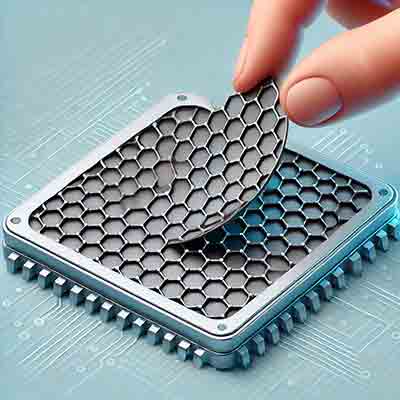
Graphene, a 2D material with exceptional electrical and optical properties, when combined with silicon wafers, enables next-generation devices in electronics, energy storage, and photonics. Below is an overview of its purpose and applications.
Purpose of Graphene and Silicon Wafers
- Graphene: Ultra-thin, highly conductive, and transparent, graphene enhances electrical and thermal performance.
- Silicon Wafers: Provide a stable, scalable platform for graphene integration using well-established fabrication techniques.
- Together, they enable advanced research and development in semiconductors, sensors, and energy devices.
Applications of Graphene on Silicon Wafers
1. Electronics
- High-speed transistors with ultra-fast switching.
- Flexible electronics for displays and wearables.
- Graphene-based interconnects for low power loss.
2. Photonics
- Ultra-sensitive photodetectors for optical communication.
- High-efficiency solar cells with improved electron mobility.
- Transparent electrodes for LEDs and touchscreens.
3. Sensors
- Gas sensors for detecting CO₂, NO₂, and ammonia.
- Biosensors for DNA, proteins, and glucose detection.
- Pressure and strain sensors with high precision.
4. Energy Storage
- Graphene-enhanced lithium-ion batteries for higher energy density.
- Supercapacitors with fast charge and discharge capabilities.
- Thermoelectric devices for energy harvesting.
5. Quantum Research
- Graphene-based quantum dots for advanced nanotechnology devices.
- Lab-on-chip devices for chemical and biological experiments.
Summary Table of Applications
| Field | Applications |
|---|---|
| Electronics | High-speed transistors, flexible devices |
| Photonics | Photodetectors, solar cells, transparent electrodes |
| Sensors | Gas sensors, biosensors, strain sensors |
| Energy Storage | Batteries, supercapacitors, thermoelectric devices |
| Quantum Research | Quantum dots, nanotechnology, lab-on-chip |